Table of Contents
ToggleBasics of Transistors
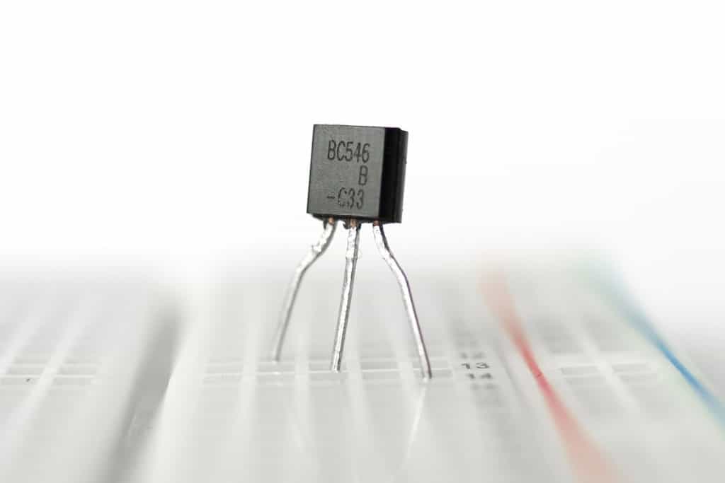
Hello Friends !! Today we are going to learn Basics of Transistors in electronics.
A transistor is composed of two pn junctions created by sandwiching either p-type or n-type semiconductor between opposite types.
There are 2 Types of Transistors:
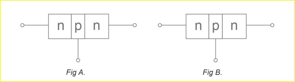
1. n-p-n transistor
2. p-n-p transistor.
An n–p–n transistor is composed of two n-type semiconductors separated by a thin section of p-type. Please refer fig A. However, a p-n-p transistor is formed by two p-sections separated by a thin section of n-type. Please refer fig B.
Here are some significant facts to consider regarding transistors:
1. Transistors are composed of two diodes placed together, which allows electrical current to flow in a controlled manner.
2. Transistors have three distinct terminals, comprising varied materials, designed to regulate the flow of electric current.
3. The thin and slender layer at the center of transistors, known as the “base,” manages the electric current’s movement, making it a critical component for the device to function properly.
Transistor Terminals
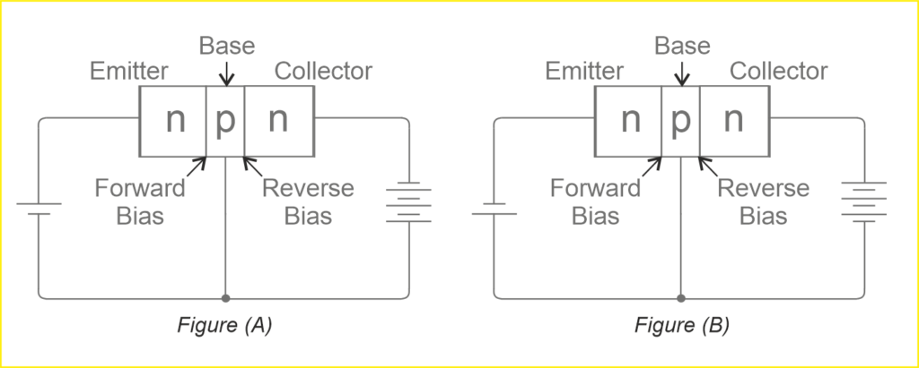
A transistor, whether pnp or npn, consists of three doped semiconductor sections. The emitter is located on one side, while the collector is positioned on the opposite side. The middle section, known as the base, forms two junctions between emitter and collector.
A) Emitter:
The section on one side, known as the emitter, is responsible for providing an abundance of charge carriers (either electrons or holes). It is always forward biased with respect to the base to facilitate the supply of a large number of majority carriers.
In Figure (A), the emitter (p-type) of a pnp transistor is forward biased, supplying hole charges to its junction with the base. Similarly, in Figure (B), the emitter (n-type) of an npn transistor is forward biased, delivering free electrons to its junction with the base.
B) Collector:
The section on the other side, known as the collector, is responsible for collecting the charges generated in the transistor. It is always reverse biased to efficiently remove charges from its junction with the base.
In Figure (A), the collector (p-type) of a pnp transistor is reverse biased and receives hole charges that flow through the output circuit. Similarly, in Figure (B), the collector (n-type) of an npn transistor is reverse biased and receives electrons.
C) Base:
The middle section of the transistor that forms two pn-junctions between the emitter and collector is known as the base.
The base-emitter junction is forward biased, creating a low resistance path for the emitter circuit. On the other hand, the base-collector junction is reverse biased, resulting in a high resistance in the collector circuit.
This differential biasing of the base junctions allows for the control of current flow and amplification in the transistor. Hope till now we learn some Basics of Transistors.
Facts about the Transistors
Before explaining how transistors work, it’s essential to have some basic knowledge about them. Keep in mind these facts about transistors:
(1) The transistor consists of three regions: the emitter, base, and collector. The base region is thinner than the emitter, while the collector region is wider. However, for simplicity, the emitter and collector are often shown to be of equal size in diagrams.
(2) The emitter is heavily doped to facilitate the injection of a large number of charge carriers into the base. The base, on the other hand, is lightly doped and very thin, allowing it to pass most of the injected charge carriers from the emitter to the collector. The collector is moderately doped.
(3) The transistor comprises two pn junctions, making it analogous to two diodes. The junction between the emitter and base is known as the emitter-base diode or simply the emitter diode. The junction between the base and collector is referred to as the collector-base diode or simply the collector diode.
(4) The emitter diode is always forward biased, meaning that a positive voltage is applied to the emitter with respect to the base. In contrast, the collector diode is always reverse biased, meaning that a negative voltage is applied to the collector with respect to the base.
(5) The resistance of the forward-biased emitter diode is very small compared to the reverse-biased collector diode. As a result, the forward bias applied to the emitter diode is typically very small, while the reverse bias applied to the collector diode is much higher.
I hope you like above blog. There is no cost associated in sharing the article in your social media.
Thanks for reading!! Happy Learning!!