
12 Essential PCB Design Rules Every Electronics Engineer Should Know
A practical, engineer to engineer walkthrough of the layout, routing, grounding, and manufacturability rules that separate a PCB that just works from one that works reliably for years.
Learn the 12 essential PCB design rules that help engineers create reliable, manufacturable, and high performance printed circuit boards. This beginner friendly guide covers layout, routing, grounding, power distribution, and signal integrity best practices.
PCB Design Rules: Introduction
A printed circuit board is the foundation of almost every electronic device you will ever build or repair, from a smartphone to an industrial PLC panel. Even when the schematic is perfect, a poorly designed PCB layout can still cause noise, signal distortion, overheating, electromagnetic interference, and manufacturing defects that show up only after the board is built.
Good PCB design is never just about connecting components with copper. It means thinking through component placement, trace routing, grounding, power distribution, thermal management, and manufacturing requirements together, not one after the other. Whether you are a student wiring your first board or an engineer shipping complex multilayer designs, these PCB design rules will help you improve performance, simplify manufacturing, and cut hours out of troubleshooting.
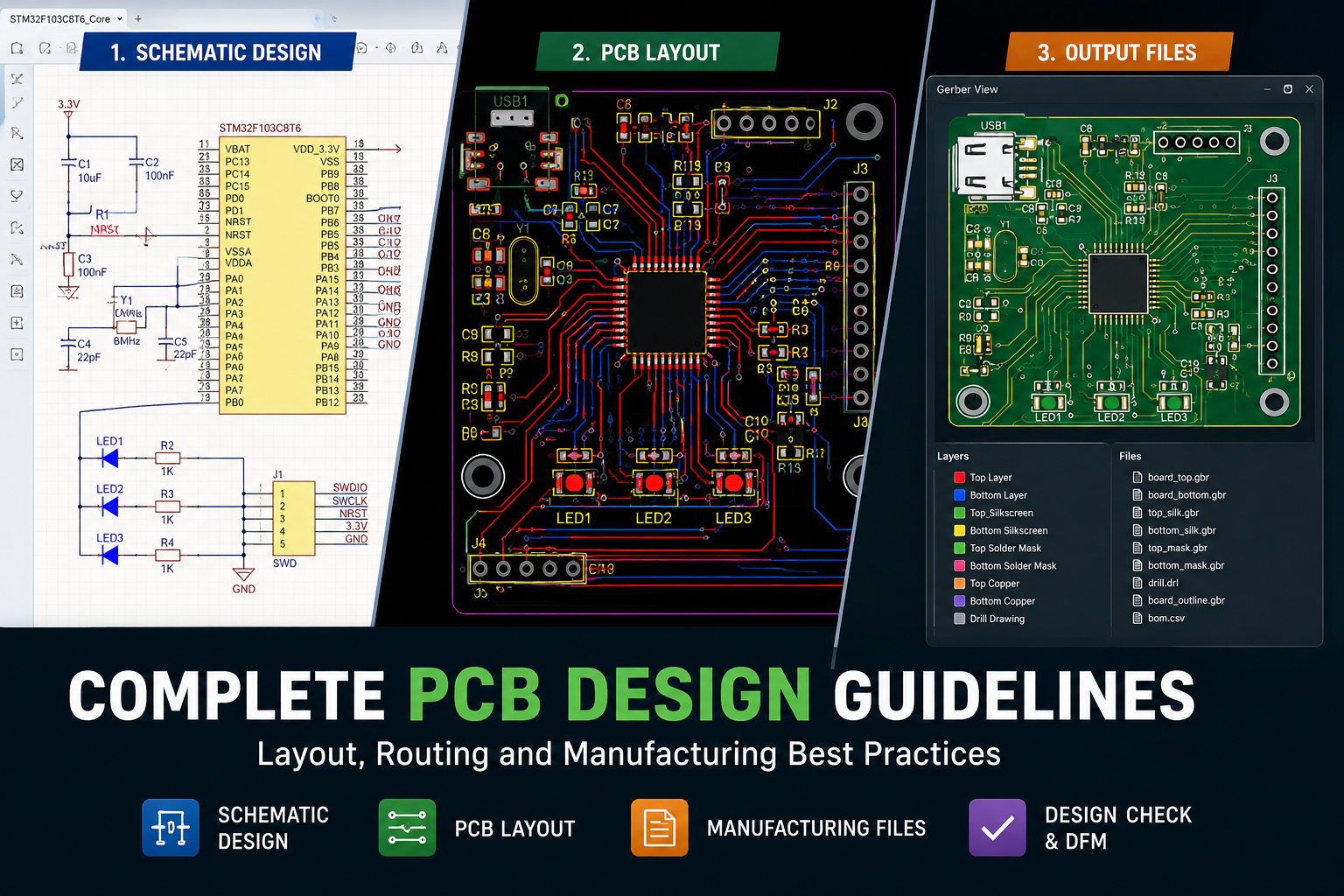
12 PCB Design Rules Every Engineer Should Follow
Place Components Logically
Group related parts, keep analog and digital sections apart, and place connectors near the edges before you route a single trace.
Keep Signal Traces Short
Shorter traces mean less resistance, less inductance, and far less chance of picking up noise.
Use a Solid Ground Plane
One continuous copper ground layer gives current a low impedance return path and cuts EMI dramatically.
Keep Power Traces Wide
Wider copper for power and ground reduces resistance, voltage drop, and unwanted heating.
Separate Analog and Digital
Keep fast switching digital noise away from sensitive analog signals in sensors, ADCs, and DACs.
Decouple Capacitors Near ICs
Place decoupling capacitors as close as possible to IC power pins to absorb switching current spikes.
Avoid Sharp Trace Corners
Use 45° bends instead of 90° corners to reduce impedance discontinuities and reflections.
Maintain Proper Trace Spacing
Keep enough distance between adjacent traces to prevent crosstalk and reduce short circuit risk.
Minimize Vias on Fast Signals
Every via adds resistance, inductance, and capacitance. Keep high speed traces on one layer where you can.
Design for Thermal Management
Give power devices and regulators enough copper area, thermal vias, and airflow to stay cool.
Follow Design for Manufacturability
Match your PCB manufacturer's spacing, drill, and pad rules so the board builds cleanly the first time.
Perform a Design Rule Check
Run DRC after placement, after routing, and again before you generate Gerber files.
Categories of PCB Design Guidelines to Plan Around
Where components sit on the board and how that shapes every trace you route afterward.
Best for: reducing routing complexity and EMI from the very first step.
Rules 1, 5How traces carry signals cleanly, without picking up or radiating noise.
Best for: high speed digital, RF, and mixed signal boards.
Rules 2, 7, 8, 9How the board delivers stable voltage and a clean return path to every IC.
Best for: preventing voltage drop, ground bounce, and false triggering.
Rules 3, 4, 6How the board survives soldering, assembly, and long term operation without failing.
Best for: production ready boards with fewer post fabrication surprises.
Rules 10, 11, 12Ground Plane and Trace Routing Concept
- Trace routed with a 90° corner, avoid this on high speed signals
- Trace routed with 45° bends, the preferred professional approach
- Continuous ground plane directly beneath the signal layer, giving return current the shortest possible path
PCB Trace Width Calculation Formula (IPC-2221)
Comparison of PCB Design Rules and Their Purpose
Applications of Reliable PCB Design
Consumer Electronics
Smartphone PCB design packs 10 to 16 layers into an area smaller than your palm.
Industrial Automation
Instrumentation PCB design relies on clean grounding to resist plant floor noise.
Automotive Systems
Automotive PCB design needs wide power traces and strong thermal management.
Medical Devices
Medical PCB design keeps signal integrity and EMI control tight where accuracy matters most.
Aerospace Electronics
Aerospace PCB design saves weight and space while surviving vibration and thermal stress.
Embedded Systems
Embedded PCB design depends on decoupling and short traces for stable operation.
PCB Design Do's and Don'ts
✅ Do This
- Place components logically before routing a single trace, this is the first rule of good PCB design
- Use one continuous ground plane wherever possible
- Keep decoupling capacitors close to IC power pins
- Route high speed traces with 45° bends, standard practice in professional PCB design
- Run a Design Rule Check after placement and after routing
❌ Avoid This
- Placing decoupling capacitors far from IC power pins
- Using narrow traces for high current paths
- Splitting the ground plane unnecessarily
- Routing high speed signals over gaps in the ground plane
- Skipping the final Design Rule Check before fabrication
PCB Trace Width Calculator
Trace Width Calculator
Based on the IPC-2221 current capacity formulaCommon PCB Design Mistakes to Avoid
Even experienced engineers repeat these PCB design mistakes. Watch for them on every PCB design review, whether you are checking your own layout or someone else's.
- Placing decoupling capacitors too far from IC power pins
- Using narrow traces on high current paths
- Splitting the ground plane without a good reason
- Routing high speed signals over gaps in the ground plane
- Mixing analog and digital circuits without proper isolation
- Ignoring thermal management until the board overheats in testing
- Skipping the final Design Rule Check before sending files to fabrication
PCB Design Video Walkthrough
PCB Design Rules FAQ
- IPC, Association Connecting Electronics Industries, IPC-2221 Generic Standard on Printed Board Design
- Cadence, Routing Traces in PCBs: Best Practices
- ALLPCB, PCB Trace Routing Design Rules for Manufacturability
What We Learn Today
- Component placement comes before routing and shapes every trace that follows
- A solid, uninterrupted ground plane is one of the highest impact PCB design rules
- Power traces need enough width, decoupling capacitors need to sit close to the IC
- 45° bends, proper trace spacing, and minimal vias protect signal integrity
- Thermal management and Design for Manufacturability decide if a good schematic becomes a reliable product
- A final Design Rule Check catches expensive mistakes before they reach fabrication